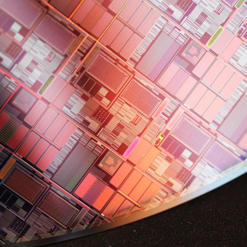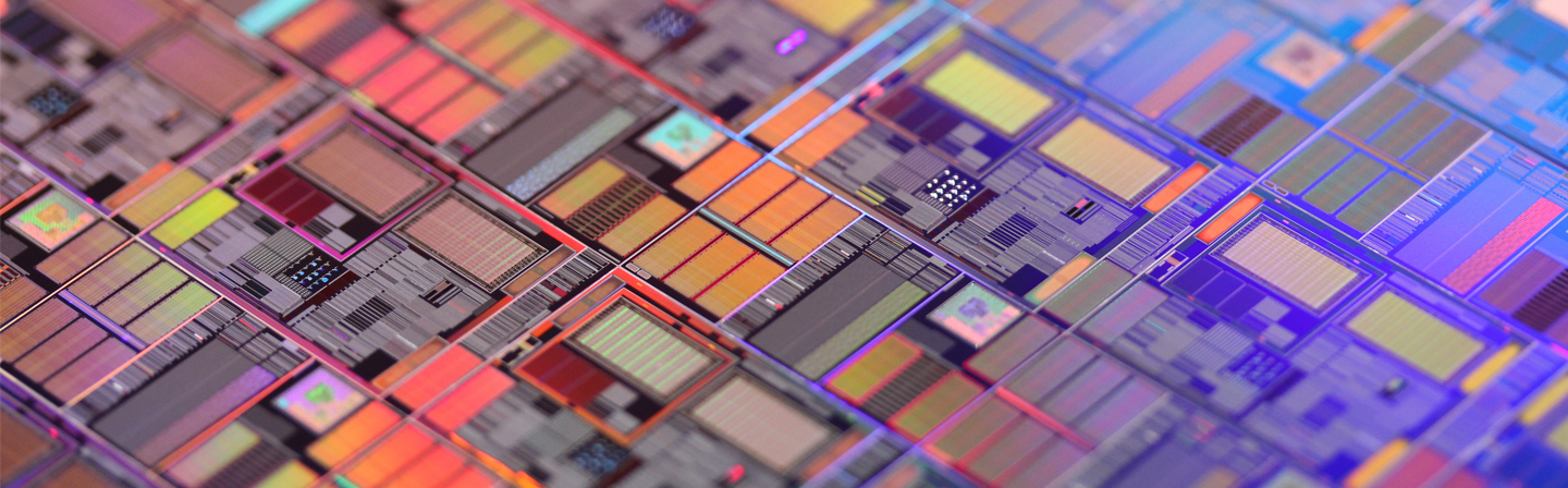
For high volume production (HVM) of semiconductor devices such as microprocessors, every single process step is of interest for evaluation and optimization. Test vehicles and test wafers are essential for testing developments and new materials under production conditions. Test wafers enable scientists to react quickly on process changes and transfer chemicals or processes from „Lab to Fab“ for HVM.
The Screening Fab at Fraunhofer IPMS is intensively researching the production and optimization of semiconductor devices and offers a multitude of advantages.