Wafer Cleaning

300 mm Screening Fab Services

© Fraunhofer IPMS
TEM images of metallization stack after TiN wet etch without (up) and with copper protection (down)

As the requirements for increased device performance and reliability have become more and more challenging in VLSI and ULSI silicon circuit technology, techniques to avoid contamination and processes to generate very clean wafer surfaces have become critically important. 

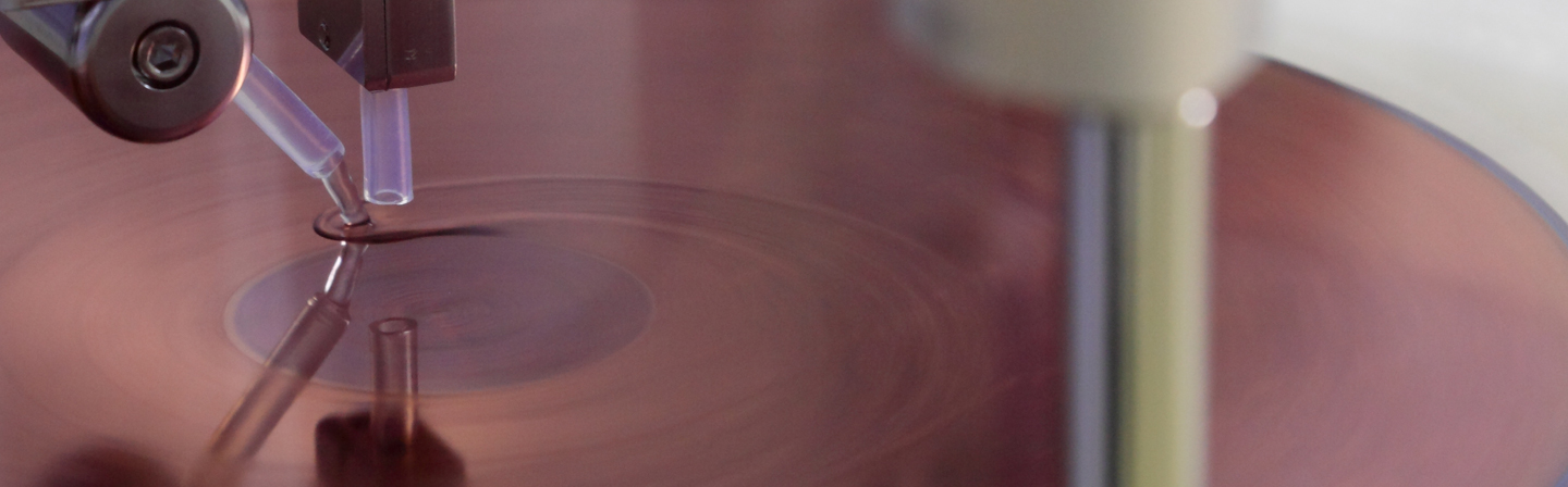
Many cleaning operations are necessary in the course of semiconductor manufacturing and must be performed at certain critical processing steps. To ensure a fast, selective, uniform and cost effective cleaning, the Center Nanoelectronic Technologies provides a state-of-the-art cleaning platform. 

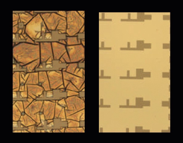
As a chain link between suppliers and fab we are able to screen, evaluate and optimize new chemicals and processes from laboratory scale up to testing on own 2x nm node test wafers. 


Applications

  • 2x nm technology node
  • From beaker test to 300 mm industry scale
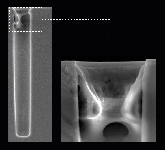
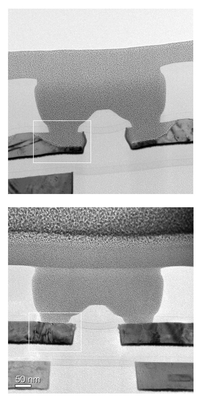
  • PostEtchResidualRemoval (PERR)
  • Photoresist stripping
  • Lithography stack rework
  • Dual damascene metal hard mask etch
  • Bath life time evaluation
  • Consumable benchmarking

Advantages

© Fraunhofer IPMS
Nanostructured sample before (left) and after photo resist removal (right).
  • Evaluation of new equipment and materials under industry standard conditions
  • AMAT Semitool Raider SP | DNS FC3000 and BREWER Science flexible labtool
  • Pre- and post-processing for optimization of individual process steps
  • Inline metrology
  • Professional contamination management
  • Professional IP management and licensing
  • Close connection to industry
  • Availability of patterned 300 mm short loop test wafers

Advantages

• Evaluation of new equipment and materials under industry standard conditions

• AMAT Semitool Raider SP2 | DNS FC3000 and BREWER Science fl exible Labtool

• Pre- and post-processing for optimization of individual process steps

• Inline metrology

• Professional contamination management

• Professional IP management and licensing

• Close connection to industry

• Availability of patterned 300 mm short loop (M1/M2 dual damascene) test wafer

Analytical Services

© Fraunhofer IPMS
Removal of passivation as well as top resist by novel phase fluids. No solvent treatment or plasma strip needed.
  • Surfscan wafer analysis (KLA Tencor SP2)
  • Patterned defect inspection (NextIn Aegis I)
  • Review SEM (Applied Materials G3 FIB)
  • 4-point resistivity measurement (KLA Tencor RS100)
  • Porosimetry (Semilab SOPRA EP5)
  • Ellipsometry (KLA Tencor FX100)
  • FIB-SEM, TEM (FEI Strata400 / FEI F20 (200 kV))
  • ToF SIMS (Ion ToF 300R)
  • Optical Microscope
  • Varian ATR-FTIR
  • AFM - Atomic force microscopy (Veeco Dimension™ X3D)
  • XPS - X-ray photoelectron spectroscopy (Thermo Fisher Scientific Theta 300i)