Nanopatterning

Nanopatterning via E-Beam Lithography

Creating nano-scale structures is necessary for a wide range of applications in the semiconductor business. Key challenges are creating precisely controlled patterns with small dimensions, flexible and adaptable layout generation and processes as well as uniform and reproducible wafer-scale integration.

E-Beam shaped conductive circuits in aluminum for DRAM applications.
© Fraunhofer IPMS
E-Beam shaped conductive circuits in aluminum for DRAM applications.
Vistec SB3050DW 50keV variable shaped e-beam for 4‘‘, 6“, 8“ & 12“ wafer sizes.
© Fraunhofer IPMS
Vistec SB3050DW 50keV variable shaped e-beam for 4‘‘, 6“, 8“ & 12“ wafer sizes in CNT cleanroom.

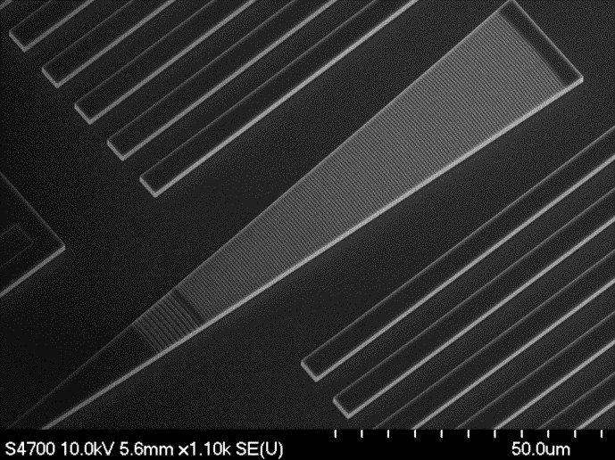
Our Screening Fab offers state-of-the-art nanopatterning capabilities using electron beam direct write lithography and reactive ion etching. Thus, customized structures with sizes down to 32 nm can be created on a variety of wafer sizes and substrate types.

Starting from the customer’s design the whole package involving layout generation and modification, data preparation, e-beam lithography, pattern transfer using etch processes together with the needed in-line metrology and analytics up to separation winto single chips is offered.


Advantages at the Center Nanoelectrionic Technologies

Realization of customer specific patterning from sketch to etch

Direct maskless patterning

Structuring without optical diffraction limit down to 32nm (half pitch)

Simultaneous exposure of various designs or layout variations on single wafer, mix&match

Different etch capabilities (ICP, CCP, high-T, MW, …)

Wide range of inline-metrology and analytics available (e.g. structure analysis via REV SEM and X-Sections)

ISO 9001 certification for professional contamination managment and high quality industrial services

Close industry connection and vast collaboration network (foundries, supplier and universities) with over 10 years of experience

Application Examples

We provide the whole process chain from customer applications to chip separation including layout and data preparation, nanopatterning and cleaning.

© Fraunhofer IPMS
© Fraunhofer IPMS / IHM Dresden
Optical coupling as designed (up) and as final imprint template (down).

Fabrication of test structures for technology development

Structuring of Application Specific Integrated Circuits (ASICS)

Future technology nodes development 

Design tests of innovative devices and cell concepts and their variation on a wafer (Chip Shuttle)

Calibration pattern for metrology development

MEMS and NEMS patterning with productive quality

“Mix & Match” with optical exposure techniques

Optical gratings and light modulation devices

Correction of design or process errors in finalized CMOS structures (Metal Fix)

High aspect ratio patterning (TSV, 3D capacitors)

Nanoimprint masters

Lithography

Vistec SB3050DW:

50keV variable shaped e-beam

Wafer sizes: 4‘‘, 6“, 8“ & 12“


TEL ACT 12 Clean Track:

Fully automated 12“ coating and development

Processing of chemically amplified resists (CAR) and non-chemically amplified resists

Additional coating of i-line, KrF and ArF available


Brewer Science CEE 100 & 200 FX 

Wafer sizes: 4‘‘, 6“, 8“ & 12“


AMAT Verity 4i CD-SEM:

Wafer sizes: 8“ & 12“


Leica INS3300 optical inspection:

Wafer sizes: 8“ & 12

Etch

2 Applied Material Centura Mainframe for 12” Wafer (BEOL and FEOL)

ICP/CCP reactor with option for high temperature etching (substrate temperature up to 250 °C)

Remote plasma 

Active OES endpoint controlling 

Optional 8“ wafer processing 

In- situ Plasma analytics viable 

Structures whit critical dimension (CD) down to few nm 

High aspect ratio etching (> 20:1) 


Etching of different materials: 

- Standard materials: Substrate Si, poly-Si, amorphous Si 

- Hard mask materials: SiN, SiO2

- Metal gate materials: TiN, TaN, W, WSi

- High-k Materials (at 250 °C): Al2O3, HfO2, SiHfOx, ZrO2

- Metal: Al, AlSi