Atomic Layer Deposition (ALD) is a thin film deposition method which is based on temporally or spatially separated surface reactions resulting in cyclic self-limiting monolayer coverage. Due to its unique characteristics like precise film thickness control, excellent uniformity and conformity as well as lower deposition temperatures compared to other CVD methods, ALD has become more and more state-of-the-art for an increasing number of applications.
300 mm ALD Center
Leading edge high-k technologies for 300 mm (12 in) and customized test and characterization services.
Atomic Layer Deposition (ALD)
300 mm Screening Fab Services
Atomic Layer Deposition (ALD) Applications
We are offering our leading edge high-k technologies for 300 mm (12 in) and smaller wafer sizes in an unique competence center for Atomic Layer Deposition - bridging the need for initial high investment for entering the field of ALD for small to large sized companies. We are addressing the needs of fast and accurate electrical results for process development or failure analysis, customized tests and characterization services on wafer level as well as the scale up of novel precursor chemistries. From early lab results to 300 mm (12 in) processing equipment that is qualified to run device wafers and support pilot ramp into manufacturing, the Screening Fab is covering all process steps.
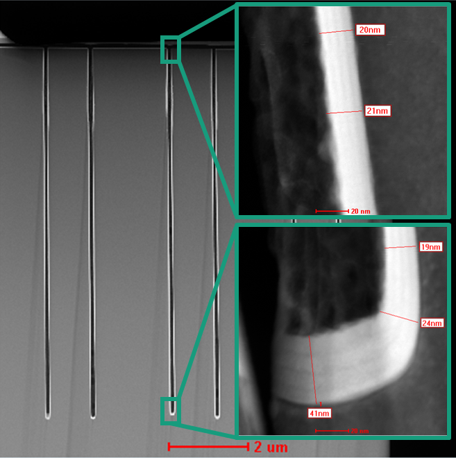
STEM analysis of a highly conformal high-k oxide laminate coating by ALD for MIM capacitor applications in high aspect ratio structures (>50:1).
- ALD deposited High-k oxides and electrodes for: stand-alone memory and embedded memory (SRAM, DRAM, RRAM and FRAM)
- HfO2, TiN and TaN for High-k / Metal Gate (HKMG) for different flavors: high-k first, high-k last, FDSOI and FinFET transistor technologies
- Fully CMOS-compatible ALD deposited HfO2 based ferroelectrics for FeFET NVM memory
- Passive components integrating ALD deposited 3D high-k MIM capacitors (for buffering and decoupling purposes in chip (System on Chip - SoC) or package (System in Package - SiP) level)
- Plasma activated ALD (PEALD) nickel for NiSi source/drain contacts
- ALD processes of metal and metal nitrides integrated in 28 nm BEOL copper interconnects
- PEALD oxide and nitrides for the transistor module and for sub 28 nm double patterning schemes such as SADP
- Hardmask for high aspect etching in silicon and oxide
- Passivation layers for photovoltaics
- ALD processes for MEMS/MOEMS applications: etch stops, wear resistant layers, optical layers (Bragg mirror) and sensor materials (ISFET)
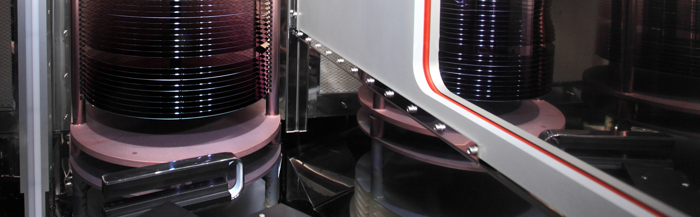
ASM ALD tool at Fraunhofer Screening Fab Dresden, Germany.
Rapid ALD precursor screening
- Fast screening by employing in-situ analytics (QCM and QMS)
- Fundamental research on nucleation fi lm growth and step coverage
- Scale up to from small samples up to 300 mm wafers
- Single wafer and Large Batch ALD
- Crossflow, Showerhead and Batch Furnace process chambers
Materials research and development for:
- High-k oxides (HfO2, ZrO2, TiO2, Al2O3 ,SiO2)
- Metals and metal nitrides
- Cu BEoL barrier/seed
- Hardmasks for high aspect ratio etching in silicon and oxide
- Liners and spacer
- Low cycle-time test chip for electrical read out for MIS / MIM devices
- Planar and 3D high-aspect ratio structures