Fraunhofer Screening Fab constantly optimizes the Electrochemical copper deposition (ECD) process and the copper material to guarantee high performance and low power signaling together with long durability. ECD processes for the galvanic deposition of metal layers through electrolyte screening, bath life time investigation and process characterization as well as electrochemical measurement methods (cyclic voltammetric stripping, electrochemical impedance spectroscopy) and extensive analytics are available at Fraunhofer Screening Fab to optimize copper superfillings.
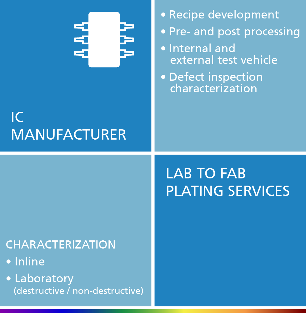
Fraunhofer Screening Fab Plating Services for IC Manufacturer
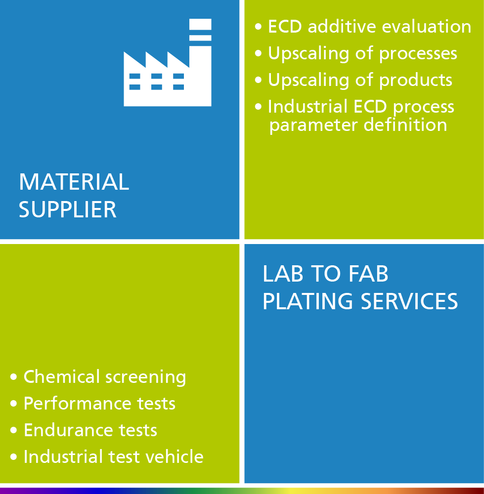
Fraunhofer Screening Fab Plating Services for Material Supplier
Advantages
- Evaluation of new equipment and materials under industry standard conditions
- Leading edge plating tools for process optimization (AMAT Semitool Raider ECD / LAM Sabre Extreme)
- Pre- and post-processing for optimization of individual process steps
- Inline metrology
- Professional contamination management
- Professional IP management and licensing
- Close connection to industry
Applications
- 28 nm technology node & below
- 300 mm/12 in wafer & beaker tests
- Dual damascene plating
- Bump plating
- TSV plating
Analytic Services
- Surfscan wafer analysis (KLA Tencor SP2)
- 4-point resistivity measurement (KLA Tencor RS100)
- High resolution profi lometry (KLA Tencor HRP340)
- Ellipsometry (KLA Tencor FX100)
- Review SEM (Applied Materials G3 FIB)
- Patterned defect inspection (NextIn Aegis I)
- FIB-SEM, TEM (FEI Strata400 / FEI F20 (200 kV))
- ToF SIMS (Ion ToF 300R)
- Electrochemical analysis (ECI QualiLab 10-EZ beaker analysis)
- Potentiostat / Galvanostat (Princeton Applied Research)