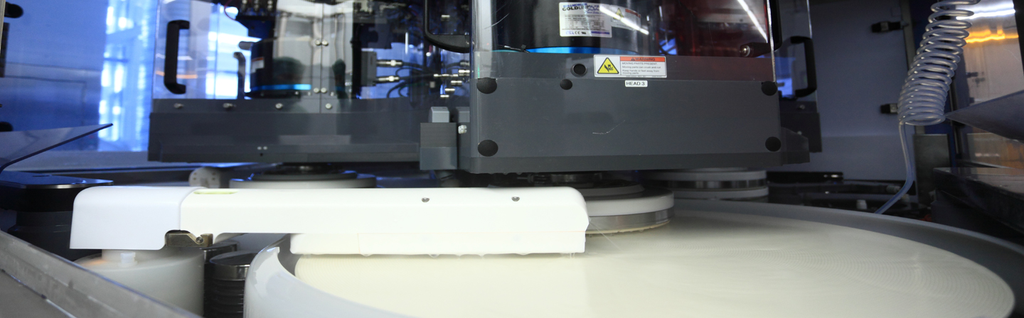
The CMP Process
Highly integrated circuits, like logic and memory chips, consist of many material layers. In the course of manufacturing the surfaces have to be planarized over and over again to obtain sufficient process windows for critical processes like lithography and etching. Furthermore planarization ensures defined sizes of the structures, thus in the end reliable functioning of the electronic elements. Chemical-mechanical planarization (CMP) is the state of the art to reach the necessary planarity. The continuous shrinking in the semiconductor technology goes along with a higher demand for accuracy, as well as a higher number of materials used. Therefore it is necessary to understand the various CMP processes and to develop novel processes for newly introduced materials to be able to fulfill the demands of the coming technology nodes.
Applications
• CMP process development and optimization
• CMP design for manufacturing strategy development with semiconductor product manufacturers
• CMP consumables screening and characterization (Polishing pad - Conditioner - Slurry - Post CMP cleaning chemistry - Brush - Filter - and more)
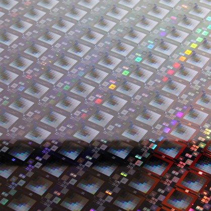
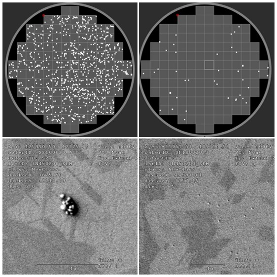
• CMP process characterization (Planarization - Defectivity - Removal rates, selectivity - Static etch rates - Electrical performance and reliability)
• Modeling and simulation of the planarization behavior of patterned wafers
• CMP wafer processing on demand